Portable Phone Power Bank
- smeltingpottutoria
- Feb 1, 2017
- 3 min read
This was a project that I put many revisions into in an effort to make a very robust and powerful phone charger that would be able to charge anyone's phone/tablet as fast as possible. There's nothing more frustrating than desperately needing to charge your phone and having a power bank that doesn't make the cut.
One of the biggest flaws with consumer grade power banks is that they are built to a strict budget. This means that manufacturers just corners when designing the boost circuit and the battery charging circuit. My goal was to over spec the phone charging circuit and design the power bank charging circuit for fast charging both ways while still considering battery safety.

Revision 2 of the power bank included 5 18650 cells and two USB ports for normal 5V charging.
Total capacity of 17Ah and 62.9 Wh.

Revision 3 included 4 18650 cells and still two USB ports, this version was the first to include support for Qualcomm quick charge 2.0 that required 9V @ 1.67Amps.
Total capacity of 13.6Ah and 50.32Wh.


Above is the first prototype lithium ion fast charging circuit. Using the LTC4002 chip for charge control, I was able to charge lithium batteries at up to 3A depending on the input supply. This circuit was then integrated into the final revision of the power bank circuit board.

Above is the final version, which is still being used. Included are six 3.4Ah 18650 cells, micro usb charging port, and three USB charging ports with one port Qualcomm 2.0 class B capable. The two right USB port share boost converter #2 for a total rate power output of 30W, while the fast charge port using converter #1 has the same 30W rated output.

Above is the final version of the second revision of the power bank board. It contains two synchronous boost converters and a lithium ion charger that can charge up to a rate of 3A. The lithium charger is based off of the LTC4002 chip. The two boost converters are based off of the TPS61088 chip. The logic for detecting a fast charge capable devices is controlled by the CHY100 IC. Fast charging is started when the CHY100 attaches another resistor (R10) into the first boost converters feedback network, switching it's output from 5V to 9V.


Final steps in the project are printing a top cover and implementing the daughter board to the main board that will monitor voltages and currents and then display them on a 1.2" OLED screen. This board will also enable the using of fast chargers to fast charge the power bank.
The Bill of Materials can be found at this link.
Daughter board prototypes
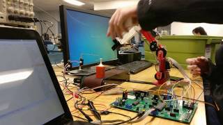
A perfboard prototype was constructed to test the various signal headers on the main boost board. The purpose of the daughter board is to display to a user, battery SOC, raw battery voltage, both output voltages from boost converters and to interface with a fast charger plugged into the charger. In order to charge the power bank at full speed using a generic samsung s7 charger, the charger must be tricked into fast charge mode, enabling the output of 9V @ 1.67Amps. In order to do this, a microcontroller (arduino nano) was configured to emulate the communication that goes on between a Qualcomm quick charge 2.0 charger and quick charge capable device. To do this a PWM signal was generated with the appropriate duty cycle and then feed into an low pass RC filter with a bandwidth low enough to generate a smooth enough signal to trick the charger. This was definitely a hack and a much better approach would be to use a DAC.

An interesting observation that was made was that a constant specific voltage on the D- and D+ connections could be made before the charger was plugged in that would put the charger in fast charge mode immediately , instead of needed to go through the whole communication cycle. With the wall charger in fast charge mode, the lithium ion charge circuit charged at a full rate of 3A. This enabled the huge power bank to be charged with a normal wall charger in around 7 hours from completely dead (~3.0v).


